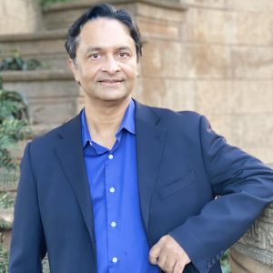
Saif Islam
Professor and Chair, Department of Electrical and Computer Engineering
Lead PI: Integrated Nanodevices and Nanosystems Research Lab
University of California – Davis, 3135 Kemper Hall, Davis, CA 95616-5270

Research Background
Professor Islam’s work has covered a broad variety of topics: ultra-fast semiconductor optoelectronics, synthesis of low-dimensional semiconductor and oxide nanostructures, and their applications in devices, ultra-sensitive novel sensors, detectors, circuits and systems; fiber optical and RF photonic communication links, and materials and devices for harsh environments. His group was the first to demonstrate light-bending and photon-trapping slow light in silicon and germanium photodetectors that capitalize on the enhanced photon-semiconductor interactions to dramatically increase the light absorption capabilities of ultra-fast semiconductor devices, overcoming their weak absorption characteristics (US patent). This demonstration has a far-reaching impact on ultra-fast integrated optoelectronic, silicon photonics, data communication, CMOS imagers, quantum sensing, computing, hardware security, energy harvesting, and disease sensing and prevention.
Dr. Islam was the first to demonstrate a semiconductor (silicon and III-V) nanowire bridging technique that effectively addresses the challenges of interfacing and integrating one-dimensional semiconductor and oxide nanomaterials in nanoelectronic and nanophotonic devices (US and International Patents). His group contributed to the progress of ultrawide-bandgap semiconductors (GaN and Ga2O3) for applications in electronics, as well as in deep-UV (solar blind) optoelectronics, charged particles-based devices for several extreme-environment applications. He demonstrated the first velocity-matched distributed balanced photodetectors with record high linear photocurrents and ultra-fast response. He also developed the technique for generating ultra-smooth metal surfaces for interfacing molecular electronic devices that improved the yield of molecular switching devices fabricated with self-assembled monolayers (SAMs) of molecules. Such metal films contributed to the smoothest superlens ever reported. His group also developed a technique for dynamically switching between positive and negative permeability of metamaterials by photoconductive coupling.
Research Interests
- CMOS-compatible silicon and III-V semiconductor-based sensors and detectors for high-bit rate data communication, telecommunication, and quantum communication;
- Imaging and sensing of faint and ultrafast signals of light, chemicals, bio-agents, pathogens, and disease;
- Novel transistors, memory, and storage devices based on group IV and wide bandgap semiconductors for standard and extreme environments;
- Cost-effective energy harvesting technologies with ultra-high efficiency.
- Theory and simulations for strengthening light-matter interactions through nanophotonic techniques for enhanced efficiency, speed, and gain in CMOS optoelectronics, imaging and sensing
- Combining photon sensing, CMOS electronics, and machine learning to enable real-time decision-making in several interdisciplinary areas of imaging, sensing and diagnostics.
- Synthesis and engineering of semiconductors and oxides for enhanced sensitivity and extraordinary durability in extreme conditions
- Understanding nanoscale and quantum phenomenon in nanodevices
- Device Expertise: Electronic and Photonic Devices, Device Physics, Semiconductor-Related Material Science.
- Design & Fabrication: System and AI on Chip Design, Advanced Semiconductor Fabrication.
- Testing & Analysis: Semiconductor Testing, Measurement, and Analysis.

