Integrated Nanodevices and Nanosystems Research (Inano)
![]()
Prof. Saif Islam’s nanotechnology research focuses on the synthesis and incorporation of low-dimensional and nanostructured materials and devices with conventional semiconductor integrated circuit (IC) elements and systems. Unlike the research-based approach of sequentially processing individual nanostructures for device physics studies, his group employs massively parallel and mass-manufacturable nanofabrication processes to reproducibly fabricate low-cost nanodevice arrays for applications in integrated nanoelectronics, ultra-fast optoelectronic, data communication, quantum sensing, computing, energy harvesting, disease sensing and prevention, and energy storage.
Inano’s Research Currently Focuses on
- CMOS compatible nanoscale silicon, and III-V semiconductor based sensors and detectors for high bit rate data communication, telecommunication and quantum communication;
- Imaging and sensing of faint signals of light, chemicals, bio-agents, pathogens and disease;
- Novel transistors, memory, storage devices and systems based on group IV and and wide bandgap semiconductors for normal and extreme environments;
- Cost-effective energy harvesting technologies with ultra-high efficiency.
1. Photon-trapping Slow-light Devices and Systems for Data and Telecom, Quantum Sensing and Solar Energy Harvesting
- Ultra-fast silicon (Si) photonics, high bit-rate data and telecommunication links, nano-optoelectronics
- Ultra-wideband and ultra-fast photodetectors/sensors with near unity efficiency
- Single photon detectors and communication links, low-light detection for LIDAR and bio-sensing, quantum communication links
- Spectrally, temporally, and spatially resolved fluorescence lifetime imaging of biomolecules
- Computational imaging system-on-a-chip, spectrometer-on-a-chip
- Visible and infrared sensors (λ = 0.8-12 μm) for imaging/sensing in security, healthcare and agriculture
- Photon trapping in III-V materials/devices for extreme bandwidth (THz) and with extreme efficiency
- Energy harvesting with extreme efficiency via photon-trapping
- Metamaterials based photonic systems
2. Nanosensors, Sensor Networks and Internet of Things (IoTs)
- Novel chemical and biological sensors, sensors for inorganic-bio interfaces
- Charged particles enabled sensors, transistors
- Nano-bridges, nanowire, and nanodot based sensors
Dr. Islam has developed two novel nano-device integration and mass-production techniques termed ‘nano-bridges‘ and ‘nano-colonnades‘ that are compatible with existing microelectronics fabrication processes. Inano develops massively parallel synthesis and integration processes for 0D and 1D nano-structures (such as semiconductors, metals, oxide, molecules etc.) for potential applications in nanoscale electronics, photonics, energy conversion, high density energy storage, bio-chemical sensors, memory, logic, MEMS/NEMS devices, 3D device/chip integration, substrate-less devices and circuit fabrication.
3. Wide Bandgap Semiconductor for Sensors, Devices and Systems
- Sensors, transistors and memory for extreme environments (extreme temperature, radiation, pressure, corrosion, vibration etc.)
- Powering devices (beta/alpha-voltaics) operating in extreme conditions
- MEMS/NEMS devices
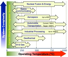
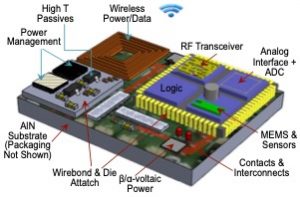
Sensors for Extreme Systems: A wide range of economic and security challenges in industry require components that operate in harsh environments, such as those found on terrestrial oil and ore extraction equipment (temperature and pressure), in vehicle engines including planes and spacecrafts (temperature and radiation), inside nuclear power plants (radiation), and industrial processing plants (corrosives). Integrated sensors that are capable of operating in extreme conditions, exhibiting exceptional thermal and chemical stability, high electrical endurance (e.g., breakdown voltage, electromagnetic shielding to survive in solar flares), very high oscillation frequency, and extraordinary reliability. These characteristics offer the potentials to design future-generation integrated systems that will allow sensors and electronics to operate in situations never before possible, thereby increasing the safety, precision, and efficiency of many machines and operating systems [Ga2O3, Wide Bandgap].
4. Nano-integrations, Nanomanufacturing, Nanoepitaxy
- Synthesis and device applications of semiconductor and oxide nanowires, nano-bridges, and nanostructures for electronics, photonics, energy conversion, energy storage
- Transistors, memory, sensors, and powering devices (batteries) enabled by the emerging nanomaterials and applications in nano-bio systems
- 3D device/chip integration, substrate-less devices, and circuit fabrication
- Self-assembly, molecular electronic devices, memristors, fundamental forces in nanodevices
Materials Systems Used: Silicon (Si), Ge, GaAs, InP, GaP, ZnO, Ga2O3, GaN, diamond, PbSe, HgCdTe
1. Light Bending and Trapping Enables Slow-Light Optoelectronics (Sensors, detectors and solar cells):
We recently demonstrated the conversion of vertically oriented light waves into an ensemble of laterally oriented collective guided modes in semiconductor thin films by integrating a 2D periodic array of nanoscale holes [1, News & Views]. Such light-bending and slowly propagating light enhance photon material interaction and dramatically increases the light absorption capabilities of semiconductors that are weak in absorption characteristics. We demonstrated silicon and germanium-based photodetectors with an order of magnitude higher quantum efficiency (QE) and bandwidth (>50 gigabit per second transmission rate with more than 60% external QE) [2-6].
1a. Highly-sensitive and Ultra-fast Detection for Optical Interconnects
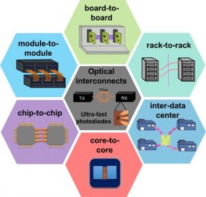
A 24 percent compound annual growth rate is estimated for global internet protocol (IP) traffic from 2016 to 2021 with a data volume of 3.3 ZB per year. The massive traffic growth is due to the next generation of wireless networks, the emergence of new cloud-computing systems, Internet of Things (IoT), and worldwide online multimedia streaming services. To handle the explosive internet traffic load, data centers are expanding rapidly with new architectures handling higher traffic volumes relative to the Internet. The amount of annual global data centers traffic in 2018 is estimated to be 11.6 ZB and by 2021 will reach 20.6 ZB, with 70% of this traffic residing within the data center. Current and future data centers are widely using low-cost and energy efficient optical interconnects. Currently, low cost, broadband, and energy efficient optical interconnects based on vertical cavity surface emitting lasers (VCSELs) and III-V materials enabled PIN (positive-intrinsic-negative) photodiodes (PDs) are widely used technologies in the high-speed optical short-reach links (<300 m) in data centers.
In general, column III-V (such as GaAs or Inx Ga1-x As) photodiodes and CMOS or SiGe amplifiers are designed and fabricated separately. Using an optimized wire bonding process, the devices are packaged together after fabrication. This method is challenging for large-scale production, and it is complicated and expensive to be used for connecting an array of photodiodes to an array of amplifiers. Moreover, undesirable packaging parasitic (such as inductance and capacitance) degrade the high-speed device performance and cause electrical crosstalk between channels. Thus, an ultra-fast silicon PD with high efficiency is very important to overcome the challenges of cost, complexity of integration and mass production.
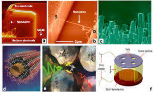
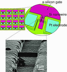
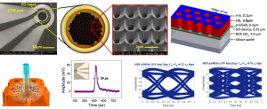
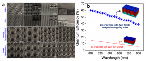
Our group recently demonstrates a silicon-based surface-illuminated CMOS compatible broadband photodiode with ≤30 picosecond full-width at half-maximum (FWHM) and high quantum efficiency at 850nm by using photon-trapping micro/nano-structures, as shown in the above Figure [1-5]. The absorption efficiency of a 2µm thin intrinsic Si layer was augmented by more than an order of magnitude and this led to more than 50% external quantum efficiency (EQE). This is the fastest reported response for a Si photodiode with such high quantum efficiency at these wavelengths. The hole array in the PD supports a set of laterally propagating slow modes that can contribute to considerably higher absorption in the PDs [1]. In these novel devices, a successful conversion of an initial incident vertical plane waves to an ensemble of lateral collective modes is realized in a 2D periodic array of holes. Strong lateral modes propagating deep into i-region enable the absorption of wide range of the wavelength and contributes to above 80% absorption. Since a PD has a much larger lateral size than its vertical thickness, lateral waves are almost completely absorbed and as a result, electron-hole pairs are efficiently generated. These generated carriers drift quickly under the strong vertical electric field in the device and create a high-speed current output.
We are now focusing on developing monolithically integrated CMOS receiver for applications in short reach optical data links [5]. While designing an integrated received using foundry services, based on the measured impulse response data of the PDs, the group simulated the eye-diagrams at 50Gb/s and 100Gb/s using their PD in computer simulations. A 1000 bits random pattern has been simulated with extinction ratio (ER)=3-dB (similar to IEEE 802.3bm) and convolved with the PD impulse response (shown in the Figure above) for these PDs. To simulate the effects of trans-impedance amplifier (TIA), the PD output is applied to a third order Butterworth filter with 3-dB bandwidth equal 0.6*Bit Rate [6]. To improve the device bandwidth, a 2-tap feed-forward pre/de-emphasis equalizers is designed and optimized in the modeling. The results (see above Figures) for 50Gb/s and 100Gb/s show that these novel highly efficient Si-based PDs have the potential to be operational up to 100Gb/s with a well-designed 2-tap pre/de-emphasis equalizers. This is more than an order of magnitude improvement for a broadband and highly efficient Si photodiode. It is anticipated that such improvement in the performance of Si PDs can contribute to dramatic cost saving in transceivers that are expected to be widely used in data center communication.
Collaborators: UCSC, NASA, US Army Night Vision and Electronic Sensors Directorate and W&W Sens
1b. High-Performance Infrared Detectors
Infrared (IR) detectors by type (Thermal IR Detector and IR Photodetector), by technology (Cooled IR Detector Technology and Uncooled IR Detector Technology), by Wavelength (Short Wave Infrared- SWIR (1.4µm – 3µm), Mid Wave Infrared-MWIR (3µm – 8µm), and Long Wave Infrared- LWIR (8µm – 15µm)) have attained a huge interest for applications in the medical, scientific, security, military, industrial, and automotive areas.
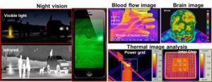
The IR imaging applications in medicine like IR thermography in neonatal thermoregulation, SWIR imaging of peripheral blood perfusion and blood vessels, MWIR and LWIR in stress imaging, emotional classification, monitoring of temperature related physiology, and medical thermal image analysis have gained much attention [1]. The IR imaging applications like IR thermography as a non-invasive technology has also gained a lot of interest in agriculture, construction, manufacturing and pharmaceutical industries for fault detection and to check the quality of an object [2].
Additionally, the increasing demand from consumer electronics applications such as tablets, smart TVs and smartphone and for security at commercial environments such as offices, hotels, airports, and hospitals plus the use of night vision ability in military and security applications are the important factors driving the IR detectors market growth. The most increasing demand is especially for use of uncooled IR technology in remote sensing, IOT and hyperspectral imaging [3].
However, the performance of IR detectors still limits to the dark current characteristics and associated noise behavior. The detectivity of IR detectors strongly depends on the operating temperature of the device, and the current IR detectors need to be cooled down even to 77K for having a low dark current. By significant reduction in dark current of IR detectors using novel device designs, they will be able to operate at sufficiently high operating temperatures (HOT) whereby their cooling systems are no longer required, providing for a reduction in cooler size, weight and power as well as overall product cost, and consequently extending their applications.
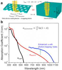
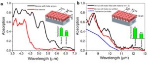
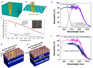
In this research, we aim at reducing the noise caused by the dark current to ensure HOT operation of the IR detectors and improve the detector quantum efficiency (QE), by using a thin absorption layer of IR absorbing materials such as mercury cadmium telluride (HgCdTe), Indium Gallium Arsenide (InGaAs) and lead selenide (PbSe). A photon bending and trapping mechanism based on integrated micro/nanoscale structures is employed to ensure high QE despite a thin absorbing layer. For instance, our research demonstrates that embedding periodic array of photon-trapping micro-holes in very thin 1.2 µm HgCdTe IR films can enhance the optical absorptions up to 80% (Figure a) and 40% (Figure b) at mid- and long-wave infrareds, respectively, which are several times higher than that in HgCdTe films without holes (flat device). The embedded periodic array of photon-trapping micro-holes not only enhances the optical absorption in IR structures but also can provide a method to reduce the material filling ratio to ~ 50%, which will lead to a significant reduction in dark current of the device, ensuring HOT operation of the IR detectors for applications in LIDAR, remote sensing and hyperspectral imaging.
Collaborators: US Army Night Vision and Electronic Sensors Directorate and Army Research Laboratory.
[1] Review of Biomedical Applications of Contactless Imaging of Neonates Using Infrared Thermography and Beyond. Methods Protoc. 2018, 1, 39. [2] Intelligent fault diagnosis of rotating machinery using infrared thermal image. Expert Systems with Applications 39.2 (2012): 2082-2091. [3] Recent progress in infrared detector technologies. Infrared Physics & Technology 54.3 (2011): 136-154.
1c. Single Photon Quantum Detectors for Extremely Low-light Detection, Communication and LIDAR
Detecting extreme levels of light is extremely critical for obtaining (i) Long range and eye safety, Light Detection and Ranging (LIDAR) systems used for autonomous cars and robotics, (ii) Extremely secure quantum communications and (iii) high resolution biomedical imaging. Single Photon Avalanche Photodetectors (SPADs) can detect extremely low levels of light since carriers generated by photon absorption undergo avalanche gain, triggering a macroscopic breakdown of the diode junction. These single photon detectors can operate at room temperature and can be fabricated in a typical silicon CMOS fabrication process, making them the most attractive photodetectors for commercial applications.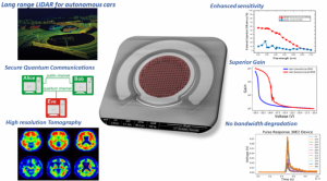 We are developing extremely sensitive SPADs incorporating photon-trapping microstructures on their surface that can bend a beam of light at 90 degrees and will allow its propagation laterally, increasing their Probability of Detection of small number of photons. This lateral propagation is exploited to enhance the Photon Detection Efficiency (PDE) of SPADs at wavelengths from the visible (400-700nm) to the Infrared (800 to 1100nm) part of the spectrum, by a direct improvement of its External Quantum Efficiency. These devices also present lower breakdown voltage (30V) compared with a regular silicon SPAD (34V), and can achieve an incredible 1000x of Gain Multiplication, all of this without degrading the bandwidth (or time response). Such SPADs promise high PDE, low jitter time and low dark count rate due to the lower excess voltage required for its operation.
1d. Solar Energy Conversion and Storage Devices (Batteries): Our work on photovoltaic devices addresses the solar-grade semiconductor scarcity (silicon and other materials) and the cost of manufacturing PV devices and panels. To this end, we fabricate devices in the shape of vertically oriented micro/nano-pillars and ridges/walls and transfer-print them to low cost, flexible and amorphous surfaces using a mass-manufacturable polymer assisted shear-fracturing process at ambient condition. This allows us to improve the efficiency and lower the costs, since the original epitaxial wafers can be repeatedly used for generating more devices. We believe that it is wasteful and environmentally detrimental to employ an expensive wafer solely for mechanically supporting a thin layer of devices. Our initial work has already demonstrated the potential of the array transfer process based on our innovative shear fracture method. This was the first demonstration of such an approach that is not dependent on any specific substrate material. The light gathering and trapping function of our micro/nano-pillar shaped devices that resemble ‘antennas’ also offers opportunities for light trapping higher efficiency in photodetectros and imaging sensors. Our group is also pursuing innovative technolgies for energy storage using silicon and similar materials as anodes in Li-ion batteries.
Multi-junction Solar Cells with Integrated Photon-trapping Nanostructures: We recently successfully demonstrated the conversion of vertically oriented light waves into an ensemble of laterally oriented collective guided modes in semiconductor thin films by integrating a 2D periodic array of nanoscale holes [Nature Photonics, 2017]. Such light-bending and slowly propagating lateral modes enhance photon material interaction and dramatically increases the light absorption capabilities of semiconductors that are weak in absorption characteristics. We demonstrated silicon and germanium-based photodetectors [Photonics Research 2018] with an order of magnitude higher quantum efficiency (QE) and bandwidth (>50 gigabit per second transmission rate with more than 60% external QE).
We are developing extremely sensitive SPADs incorporating photon-trapping microstructures on their surface that can bend a beam of light at 90 degrees and will allow its propagation laterally, increasing their Probability of Detection of small number of photons. This lateral propagation is exploited to enhance the Photon Detection Efficiency (PDE) of SPADs at wavelengths from the visible (400-700nm) to the Infrared (800 to 1100nm) part of the spectrum, by a direct improvement of its External Quantum Efficiency. These devices also present lower breakdown voltage (30V) compared with a regular silicon SPAD (34V), and can achieve an incredible 1000x of Gain Multiplication, all of this without degrading the bandwidth (or time response). Such SPADs promise high PDE, low jitter time and low dark count rate due to the lower excess voltage required for its operation.
1d. Solar Energy Conversion and Storage Devices (Batteries): Our work on photovoltaic devices addresses the solar-grade semiconductor scarcity (silicon and other materials) and the cost of manufacturing PV devices and panels. To this end, we fabricate devices in the shape of vertically oriented micro/nano-pillars and ridges/walls and transfer-print them to low cost, flexible and amorphous surfaces using a mass-manufacturable polymer assisted shear-fracturing process at ambient condition. This allows us to improve the efficiency and lower the costs, since the original epitaxial wafers can be repeatedly used for generating more devices. We believe that it is wasteful and environmentally detrimental to employ an expensive wafer solely for mechanically supporting a thin layer of devices. Our initial work has already demonstrated the potential of the array transfer process based on our innovative shear fracture method. This was the first demonstration of such an approach that is not dependent on any specific substrate material. The light gathering and trapping function of our micro/nano-pillar shaped devices that resemble ‘antennas’ also offers opportunities for light trapping higher efficiency in photodetectros and imaging sensors. Our group is also pursuing innovative technolgies for energy storage using silicon and similar materials as anodes in Li-ion batteries.
Multi-junction Solar Cells with Integrated Photon-trapping Nanostructures: We recently successfully demonstrated the conversion of vertically oriented light waves into an ensemble of laterally oriented collective guided modes in semiconductor thin films by integrating a 2D periodic array of nanoscale holes [Nature Photonics, 2017]. Such light-bending and slowly propagating lateral modes enhance photon material interaction and dramatically increases the light absorption capabilities of semiconductors that are weak in absorption characteristics. We demonstrated silicon and germanium-based photodetectors [Photonics Research 2018] with an order of magnitude higher quantum efficiency (QE) and bandwidth (>50 gigabit per second transmission rate with more than 60% external QE).
Facilities and Resources
Inano built capabilities in three areas crucial for the projects:(1) Si epitaxial material growth (CVD/MOCVD) capability with a state-of-the-art equipment ( for Si and Ge); (2) extensive experience and resources for device design, modeling, simulation, especially for sensors, photodiodes, transistors, memory, logic and photovoltaic, and (3) device characterization. The Lab has a collection of large number of equipment for the characterization of a wide range of semiconductor devices that broadly fall under four categories: (i) Optoelectronic devices such as quantum photon detectors, (ii) Electrical device such as sensors and transistors for extreme conditions, (iii) High-speed devices and systems such as ultra-fast data receiver, and (iv) Ultra-high vacuum electronics such as charged ions based sensors. The group is also equipped with simulation tools such as COMSOL, Lumerical and several Cadence and Mentor Graphics tools.
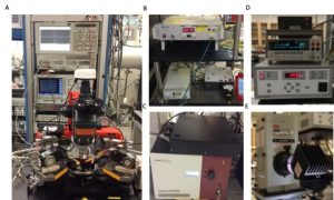
The device fabrication is carried out in the Center for Nano and Micro Manufacturing (CNM2) located at UC Davis campus. The CNM2 has a large nano-fabrication facility with a wide range of state-of-the-art semiconductor processing equipment. In addition, the Materials Science Electron Microscopy Center and Spectral Imaging Facility (SIF) in UC Davis provide all kinds of sophisticated characterization equipment such as SEM, HRTEM, EDX, and micro-Raman etc.